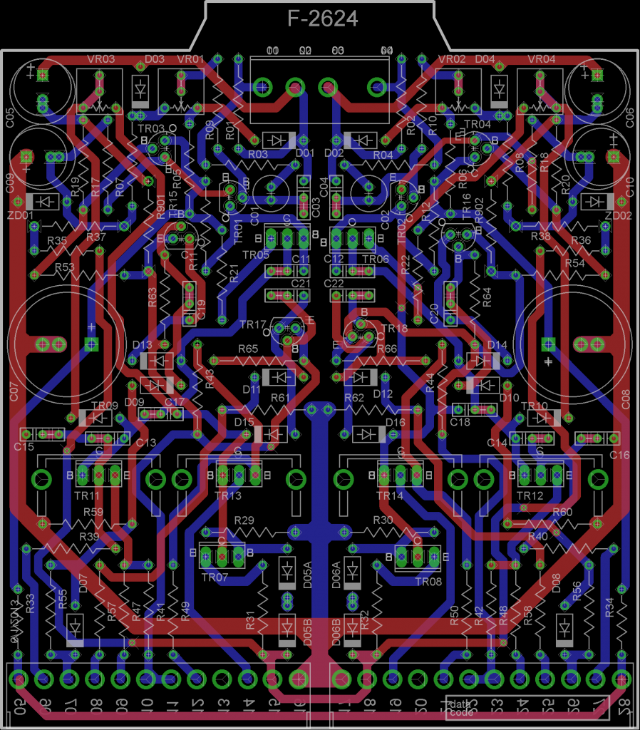
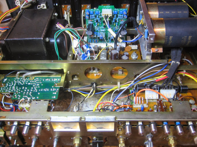
Like any vintage audio equipment user knows, one of the main issues of having such gear is the occasional problem that will need fixing. This project started because of one of these problem. As part of a discussion on another internet forum, one forum member (lets call him Tom :)) approached me and asked if I would be interested in helping him sort out a problem with a Sansui 9090DB receiver. This is a fairly old, but highly regarded piece of audio gear. The problem he described was the main amplifier board, named F2624, which is also shared with a few other Sansui models. These boards became unreliable over the years, with problematic traces, difficult to obtain parts, and so on. At the time I was just a M.Sc. student and had the free time to do things just for fun, so I jumped aboard. Following a short discussion we’ve agreed we will aim at creating a whole new board, that will be a plug-in replacement for the original F2624, but with modern parts.
The first step, was obviously getting a hold of the schematic. However, as it turns out, it doesn’t really exist anywhere that I know of. This is because the schematic that was published in the Sansui service manual was of an early version of the board, and had a couple of mistakes in it. So what do you do when you can’t get the original schematic? You draw one yourself. So that is exactly what I did, by getting an original Sansui board, and going over it. Again, as far as I know, this is the only complete schematic of this board version that is available online. Therefore, I would like to share it with others who might need it one day to repair such a board. We (myself, and Tom) have already published this on 2 internet forums to make it available to anyone who needs it. I will also include it as an attachment at the end of this post.

Once the complete schematic was drawn, next step was to find a modern replacement for each of the parts. Luckily, Tom was already familiar with this circuit and had a few “recommended” replacements for some of the parts. Most of the remaining parts took a few hours of parametric search on Mouser’s catalog to replace. However, there was still one part that didn’t have a modern replacement. That is the STV-3H triple diode. Sansui used this as part of the biasing circuit, and mounted it to the heatsink of the driver transistor for some thermal tracking.
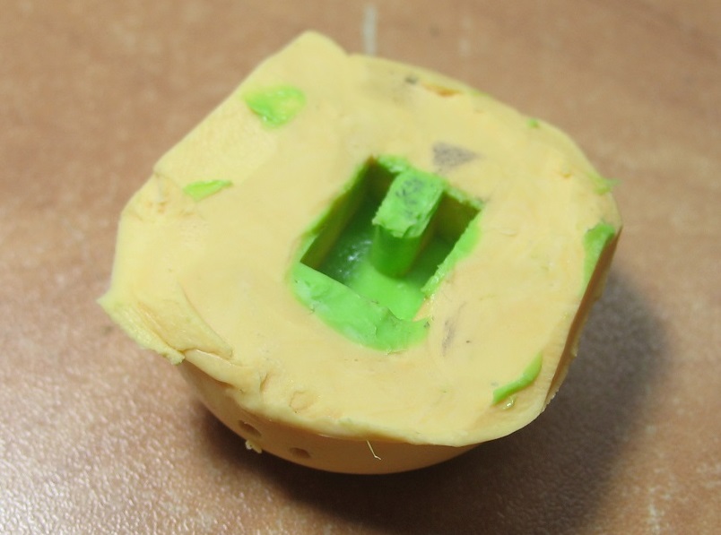
Finding original parts is still possible, although it can be a bit on the pricey side. There’s also the possibility of forgoing this partial thermal tracking. However, to try and find a solution that will be closer to the original, I’ve decided to measure a few diodes temperature-coefficient, and find something that is close enough to the original part. So far for the easy part, next I had to case this in something that will be of a similar shape and size as the original part. The solution for this was to use a silicon that is suitable for mold forming and remains fairly flexible:

To create a replacement, first 3 diodes are soldered in series, along with leads (which will come out the holes at the bottom of the mold), then it is filled with JB-weld. JB-weld is a fairly useful material which when set will conduct thermally, but will be an electrical insulator. It was a great match for this application. Finally, once the material is set, the new “triple diode” can be taken out and slightly sanded to give it a smoother finish. On the left is the original STV-3H, on the right is the new replacement:

Now that all parts had a proper replacement, with known footprints, I moved on to the board layout. This must of course be identical to the original board as far as dimension go, as it is meant to be a drop-in replacement. While doing this I’ve added a few things that are meant to be useful when assembling/working with the new board. These include:
- 2-layer PCB, no need for air-wiring like the original board
- MLCC’s support 2.5mm and 5mm lead-spacing
- Electrolytic’s support 5mm and 7.5mm lead-spacing
- Trimmers footprint support 2.5mm and 5mm wiper distance
- D05/06 now have footprint for 2 silicon diodes, no air-wiring needed
- Detailed silk-screen top (part #, EBC marking for BJT’s, polarity marks for capacitors and diodes), and bottom (EBC marking for BJT’s, polarity marks for capacitors, pin numbers on all headers)

It was now time to send the boards to print, and get them back to start testing. As always when testing something out for the first time, I’ve started with a “minimum risk” build of only half a board (1-channel), and hooked it up to a lab power-supply with a current limit, and a function generator to drive the input signal. Later on it was hooked up to a “dummy” output stage with a pair of complementary BJT’s, and resistive load. At the time I had quite limited test gear, and it took almost all of it to test this board:

The measurement results were quite good, it all worked as expected. There were a couple of things that needed attention in the next board revision, but they were mostly cosmetic. For instance, I’ve made a mistake in the footprint of the input signal connector, which meant it was larger than I’ve expected, and one of the resistors had to be moved to the bottom side of the board. Lucky for me, this is a very quick and simple fix. At this point I’ve finished assembling the board, measured the second channel to verify there aren’t mistakes there, and sent it over to Tom, for some 9090DB testing. Tom got the board, and put it into his (heavily modified) 9090DB, re-adjusting the trimmers before taking it on for a test-drive:

I won’t go into too much detail (it was also covered in his AudioKarma post), but Tom was quite happy with the sound. So we’ve decided it was time to share this with other forum members, and have 1-2 of them test out a board too, to give us some more feedback. This was a very important step, as we did get useful feedback. One of them said he could not get it to very high power levels without the signal clipping. Therefore I borrowed a 9090DB from Tom to test this, and indeed it turned out to be an actual problem. The transistor in the current limit circuit has a “C” suffix in its name, which meant it had a different pinout than the part number I was planning on using, and caused the current limit circuit to conduct despite it not being needed.
This, along with some feedback we got of what people “would like to see” in such a board, led to a new version of the PCB that had a couple of modifications, including some changes to the BOM. However, the most prominent change was an introduction of 2 LED’s into the circuit. These LED’s aren’t there to shine a light, in fact, if they light up, you are doing something wrong. They are actually there to protect the amplifiers output transistors:

These LED’s are chosen for their forward voltage drop, and they are placed in parallel with the biasing circuit. Some of the feedback I received was that some older trimmers can “open” when they are being adjusted, which has damaged output transistors on original 9090DB amplifiers. Therefore, to prevent this, the LED’s are placed in parallel. In case of an open in the quiescent current adjustment trimmer, these LED’s will limit the output voltage, and therefore current. I can happily say that in the time that has passed since I’ve added these protection elements, I have received positive feedback from several people who have made errors when servicing their amplifiers, and these LED’s saved the output stage transistors. Obviously, these LED’s are optional, and can be omitted if you don’t like LED’s in your vintage gear.

Over the last few years since I’ve created this replacement board, quite a few people have used these to repair or upgrade their 9090DB’s, as well as other Sansui gear that use the same board. This is exactly what I’ve hoped would happen, and I’m happy it helped other vintage gear enthusiasts. In the hope it will help others, I’m attaching here a zip file containing the final schematic, as well as the recommended BOM. You can obviously use other parts if you prefer, and use the default parts simply to tell you the size that will match the board footprint.
NOTE (added 4/4/21): I’ve recently been made aware of knock-off PCB’s that were sold on eBay using information that Tom and myself have created in the past. This was more than just building upon the information we’ve shared online, which is obviously available to all as we’ve intended it to be. Instead the listing was linking to Tom’s personal Google Drive schematic/BOM files and the listing content (text and photos) Tom has used in the past.
On top of that, these boards are actually different from the boards shown in this post, which only makes using these pictures and description worse as they don’t match.
To clarify, these boards aren’t being offered by us, and neither me nor Tom have anything to do with these listings.


Nicely told Toli, very nice!!! It’s 2019 now, there’s about 100 V2 F2624 out there worldwide from Brazil to Canada. So far, AFAIK, no complaints. It sounds amazing and a benchmark done by our friend Doug Brewster in the UK gave him 160W p/c. Many techs got this new PCB for their clients, including for QRX9001 units, 8080DB’s as well as 9090DB’s. It brought to life many a good Sansui units. Well done!!!
I stumbled across this thread whilst looking for something else.
Plus 1 to everything Tom S said above and I’d also like to say that the manufacturing quality of the pcb is super. I’ve assembled about six or eight (forget now) of these boards now and they’re a delight to work with; never had a lifted trace even after multiple removals/re-installations when fault finding assembly errors…
Ciao a tutti, dove si possono comprare i pcb di cui si parla? Grazie
Hi, where I could buy the pcb that you are talking about? Thank you
Hi Mario,
Please sent me an email via the contact page.
Thanks.